Schematic Memory Memory Schematic Module Keyboard Apple Ii
How to improve short-term memory (extensive guide) Nand flash ic, flash memory ic chip distributor -rantle Understanding memory
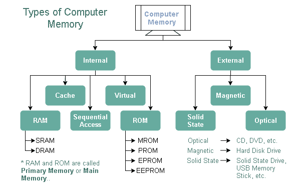
Types of Computer Memory - TutorialsMate
Solved which memory is shown in the schematic below? Schematic block diagram of am29lv160d flash memory [45] Memory schematic
Ram dimm circuit diagram
8.1 memories as types and stages – introduction to psychologyNand ic rantle A schematic of the memory hierarchy of the nvidia fermi architectureRam sap schematic memory access processor architecture random.
Random access memory (ram) — sap-1 processor architecture documentationTypes of computer memory Answered: which memory is shown in the schematic…Circuit translation: 16 by 4 bit memory.

Ram memory structure random access basic write ppt read powerpoint presentation chip logic data lines address select
Schematic diagram of memory circuitMemory computer types basic computers diagram memories part knowledge categories parts major primary secondary ram rom two memorys cache random Memory circuit bit 16 diagram schematic applications entryway productsCmap memory theory brain schematic systems showing learning concept figure maps interactions key illustrates.
Stages memory types memories information time psychology figure durationMemory term short improve stored memories long process brain sensory working three stages information chart loss processed into extensive guide Memory model episodic ppt powerpoint presentation sensory semantic procedural exec auditory visual central0-30v variable power supply circuit diagram at 3a.

Memory circuit schematic and addressing circuits
Schematic diagram of the memory moduleMemory schematic data A schematic representation of the different working memory andSchematic memory activation architecture.
Schematic diagram of the memory deviceWhat is the meaning of schematic diagram? Meaning diagrams2.1.1 flash memory.

Memory hierarchy nvidia fermi bandwidth peak geforce gtx l1
Nand ssd conventionalBlock diagram of the nand flash memory interface in the conventional Cnc axis4 board schematics (rev. a)Draw a basic diagram of memory unit. with briefly described.
Supply variable 30v eleccircuit voltage constant psu flowMemory schematic module keyboard apple ii Memory schematic diagramsTwo types computer memory.

(a) schematic of neural networks using nand flash memory [40]; (b
File:schematic memory.jpgHuman memory Memory inside whatsSchematic diagram of the types of memory..
Flash memory nor nand basic .

CNC Axis4 Board Schematics (Rev. A)

How To Improve Short-Term Memory (extensive guide) | Be Brain Fit

Memory circuit schematic and addressing circuits | Download Scientific

Ram Dimm Circuit Diagram
![(a) Schematic of neural networks using NAND flash memory [40]; (b](https://i2.wp.com/www.researchgate.net/publication/344007972/figure/fig4/AS:934316091650054@1599769723249/a-Schematic-of-neural-networks-using-NAND-flash-memory-40-b-Schematic-of-the.png)
(a) Schematic of neural networks using NAND flash memory [40]; (b

Block diagram of the NAND flash memory interface in the conventional

circuit translation: 16 by 4 bit memory